
Monolayer Graphene on SiO2/Si Substrate
Size: 3″, Grain Size: 6-10 µm
Technical Properties of Graphene Film: | |
| Transparency | > 95 % |
| Coverage | > 93% |
| Thickness (theoretical) | 0.340 nm |
| Sheet Resistance | 500-530 Ω/sq |
| Grain size | 6-10 µm |
Technical Properties of SiO2/Si Substrate: | |
| Size (inch) | 3” |
| Dry Oxide Thickness | 300 nm |
| Type | Phosphor doped / N type |
| Orientation | <100> |
| Resistivity | 0.001 – 0.01 |
| Thickness | 525 +/- 20 µm |
| Front surface | One Side Polished |
Applications:
Graphene research; Supercapacitors; Catalyst; Solar energy; Graphene optoelectronics, plasmonics and nanophotonics;
Graphene semiconductor chips; Conductive graphene film; Graphene computer memory; Biomaterials and Bioelectronics.
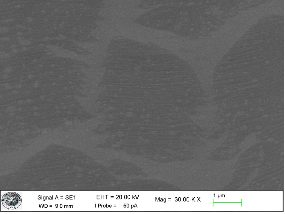
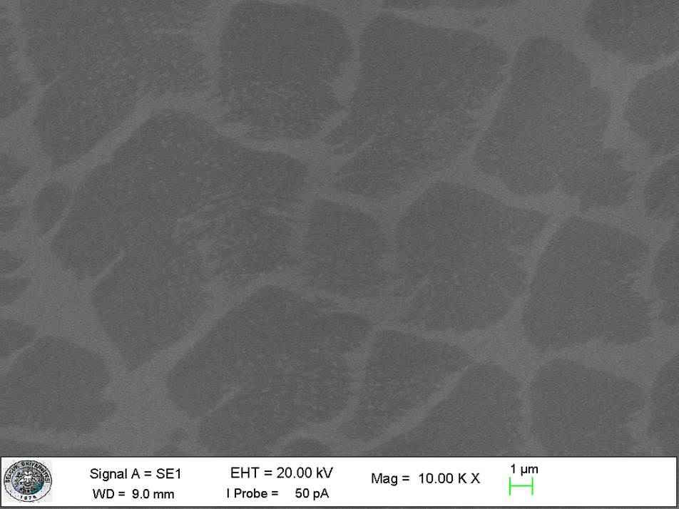
SEM Image of Monolayer Graphene

Raman Image Of Monolayer Graphene
Method of Preparation Graphene on Si/SiO2 Substrate?was prepared by the following steps: |
| 1) Single layer graphene grown on copper foil |
| 2) Deposit PMMA and curing process |
| 3) Remove Cu by etching process |
| 4) Wash PMMA/Graphene in DI water |
| 5) Redeposit PMMA/Graphene onto Si substrate and curing process |
| 6) Remove PMMA with aceton |